8-Inch P-Type Silicon Wafer with 1-100Ω Oxide Layer: Specifications and Applications、
Introduction
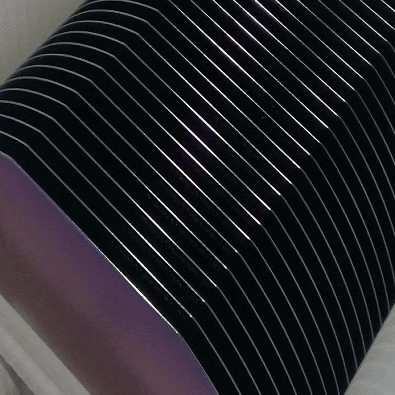
The 8-inch P-Type Silicon Wafer with a 1-100Ω oxide layer is a versatile semiconductor substrate widely used in device prototyping, MEMS production, and mid-volume electronics manufacturing. Combining boron doping for precise electrical control and a thermally grown silicon oxide (SiO₂) layer for surface passivation, this wafer balances cost efficiency with performance, making it ideal for both research and industrial applications.
Key Features
P-Type Boron Doping
Provides hole-dominated conductivity, essential for CMOS circuits, power MOSFETs, and analog devices.
Resistivity range (1~100Ω·cm) supports applications from low-power sensors to high-current power modules.
Oxide Layer (SiO₂)
Thickness Options: 10 nm to 2 μm, tailored for insulation, passivation, or as a dielectric layer.
Functions:
Reduces surface recombination and contamination.
Enhances device reliability in harsh environments.
Acts as a mask during etching or ion implantation.
Surface Quality
Single-Sided Polishing: A mirror finish (Ra < 0.5 nm) ensures precision in lithography and thin-film deposition.
Dust-Free Handling: Manufactured in controlled environments to minimize particulate defects.
Prototyping and R&D
Cost-effective for testing new device architectures due to its smaller size (8-inch) and lower material waste.
Technical Specifications
Diameter: 8 inches (200 mm)
Thickness: ~725 μm (standard)
Resistivity: 1~100Ω·cm (customizable)
Oxide Layer Thickness: 10 nm to 2 μm
Surface Finish: Single-side polished (SSP)
Oxygen Content: < 18 ppma (ASTM standards)
Advantages of 8-Inch P-Type Oxide Wafers
Cost Efficiency
Lower production costs compared to 12-inch wafers, ideal for medium-scale fabrication and academic labs.
Compatibility
Widely compatible with legacy 8-inch fabrication tools, reducing equipment upgrade costs.
Defect Control
Advanced polishing and oxide growth techniques minimize surface defects and ensure high process yield.
Flexibility
Suitable for diverse processes, including dry etching, chemical vapor deposition (CVD), and ion implantation.
Market Trends
Demand Growth: The 8-inch wafer market remains robust, driven by IoT, automotive electronics, and legacy semiconductor production lines.
Localization Efforts: China’s semiconductor industry is expanding 8-inch wafer production to reduce reliance on imports.
Sustainability: Recyclability of test-grade wafers aligns with green manufacturing initiatives.
Why Choose 8-Inch Wafers?
Balanced Throughput: Optimized for mid-volume production, offering faster turnaround times than 12-inch alternatives.
R&D-Friendly: Smaller size reduces material costs for iterative testing and academic projects.
Proven Reliability: Decades of industrial use ensure mature fabrication protocols and consistent quality.
Conclusion
The 8-inch P-Type Silicon Wafer with a 1-100Ω oxide layer is a cornerstone of semiconductor innovation, bridging the gap between R&D and industrial production. Its adaptability to CMOS, power devices, and MEMS applications,