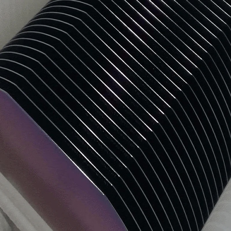
12-Inch P-Type Silicon Wafer with 1-100Ω Oxide Layer: Key Features and Applications in Semiconductor Manufacturing
Introduction
The 12-inch P-Type Silicon Wafer with a 1~100Ω oxide layer is a foundational material in modern semiconductor manufacturing. Combining high-purity P-type doping, precise resistivity control, and a thermally grown oxide layer, this substrate is essential for producing integrated circuits (ICs), power devices, and MEMS sensors. Its large diameter (300 mm) enables cost-effective mass production while meeting stringent requirements for uniformity and defect control16.
Key Specifications and Features
Material and Doping
P-Type Silicon: Doped with boron to create hole-dominated conductivity, optimized for CMOS processes and power electronics8.
Resistivity Range: 1~100Ω·cm, balancing electrical performance for applications such as analog circuits and high-voltage devices36.
Oxide Layer (SiO₂)
Thickness Options: Ranging from 25 nm to 6 μm, tailored for specific functions like insulation, passivation, or gate dielectric layers in MOSFETs39.
Functionality: Protects the silicon surface from contamination, reduces leakage currents, and enhances device reliability6.
Surface Quality
Single-Sided Polishing: A mirror-polished surface ensures precision in photolithography, while the unpolished side provides mechanical stability during fabrication13.
Manufacturing and Process Advantages
High-Purity Production
Produced via the Czochralski (CZ) method, ensuring single-crystal silicon with minimal oxygen content and radial uniformity6.
Advanced defect control techniques meet the stringent requirements of 12-inch wafer production1.
CMOS Compatibility
P-type substrates simplify CMOS fabrication by enabling direct integration of n-type MOSFETs and n-well structures for pMOS devices8.
Lower intrinsic noise and better thermal stability compared to n-type wafers8.
Cost Efficiency
The 12-inch format maximizes die yield per wafer, reducing production costs by ~30% compared to smaller diameters46.
Market Trends and Future Outlook
Growing Demand: The global 12-inch wafer market is projected to expand significantly, driven by advancements in AI, 5G, and IoT devices4.
Technological Breakthroughs: Recent innovations in China, such as 12-inch 2D semiconductor wafer production, highlight the push for next-generation materials27.
Supply Chain Resilience: With China’s semiconductor equipment market nearing 200 billion RMB, domestic production of high-quality wafers is accelerating47.
Why Choose 12-Inch P-Type Wafers?
Scalability: Compatible with both legacy 8-inch and advanced 12-inch fabrication tools4.
Uniformity: Tight control over oxygen content, resistivity, and oxide thickness ensures high device yield16.
Versatility: Supports diverse processes, including CVD, ion implantation, and dry etching39.
Conclusion
The 12-inch P-Type Silicon Wafer with a 1~100Ω oxide layer is a cornerstone of semiconductor innovation, offering unmatched performance for high-density ICs, power devices, and MEMS. As the industry shifts toward larger wafers and advanced materials, this substrate will remain vital for meeting the demands of next-generation electronics. For detailed technical specifications or procurement inquiries, consult manufacturers like Zoolied or Topvendor, which specialize in customizable oxide-layer wafers13.


