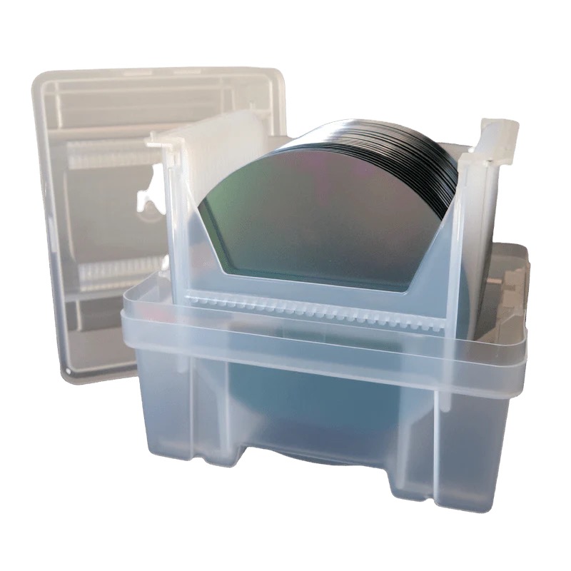
ShinEtsu 8-Inch P-Type 1~100Ω Single-Sided Polished Test Grade Silicon Wafer: Features and Applications
Introduction
The ShinEtsu 8-Inch P-Type 1~100Ω Single-Sided Polished Test Grade Silicon Wafer is a specialized substrate designed for semiconductor research, testing, and prototyping. With controlled resistivity, boron doping, and a polished surface optimized for lithography, this wafer balances cost-efficiency and performance for non-production applications23.
Key Features
P-Type Boron Doping
Doped with boron to create positive charge carriers (holes), enabling precise control over electrical properties for semiconductor device testing3.
1~100Ω Resistivity Range
Tailored resistivity supports applications ranging from low-power sensors to high-current prototypes, offering flexibility in experimental setups23.
Single-Sided Polishing
One side is mirror-polished for photolithography and thin-film deposition, while the unpolished side ensures mechanical stability during handling2.
Test Grade Quality
Designed for R&D and prototyping, this wafer prioritizes cost-effectiveness over production-grade purity, making it ideal for iterative testing and validation23.
Advantages of Test Grade Wafers
Cost Efficiency: Lower production costs compared to prime-grade wafers, ideal for budget-constrained projects3.
Defect Tolerance: Accepts minor surface imperfections, reducing waste during experimental phases2.
Scalability: The 8-inch diameter balances compatibility with legacy equipment and moderate production throughput3.
Technical Specifications
Diameter: 8 inches (200 mm)
Thickness: Standard ~725 μm (varies by ShinEtsu specifications)
Surface Finish: Single-sided polished (Ra < 0.5 nm)
Oxygen/Carbon Content: Complies with industry standards for test-grade substrates23.
Why Choose ShinEtsu?
ShinEtsu is a leader in silicon wafer technology, known for:
Consistency: Tight control over doping uniformity and resistivity.
Customization: Options for tailored resistivity and surface treatments.
Global Support: Extensive technical documentation and customer service23.
Conclusion
The ShinEtsu 8-Inch P-Type 1~100Ω Single-Sided Polished Test Grade Silicon Wafer is a versatile solution for semiconductor development. Its balance of performance, affordability, and adaptability makes it indispensable for researchers and engineers focused on innovation. For detailed technical data or procurement inquiries, refer to ShinEtsu’s official specifications or authorized distributors.