8-Inch P/N Type 1~100Ω Dust-Free Single-Sided Polished Silicon Wafer: A Versatile Semiconductor Substrate
Introduction
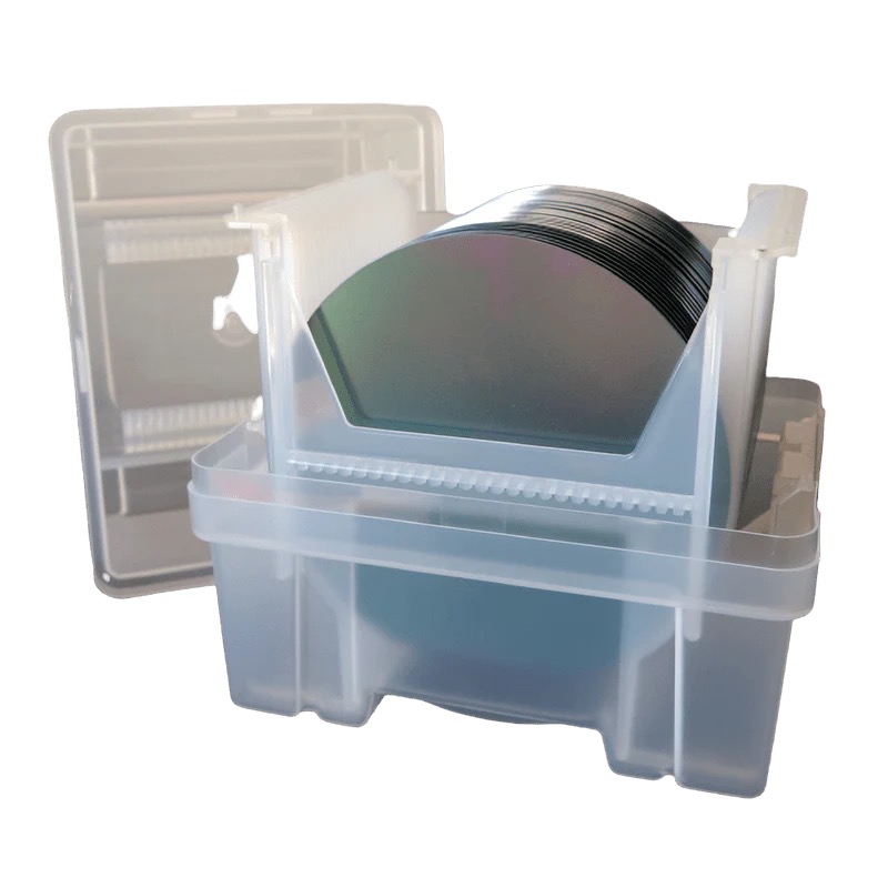
The 8-inch P/N Type 1~100Ω Dust-Free Single-Sided Polished Silicon Wafer is a high-performance substrate tailored for precision semiconductor applications. Combining controlled resistivity, pristine surface quality, and optimized electrical properties, this wafer is a cornerstone in modern electronics manufacturing, from power devices to MEMS sensors.
Key Features of the 8-Inch P/N Type Silicon Wafer
P/N Type Doping Options
P-Type Wafers: Doped with boron (B) for positive charge carriers (holes), ideal for power devices and analog circuits.
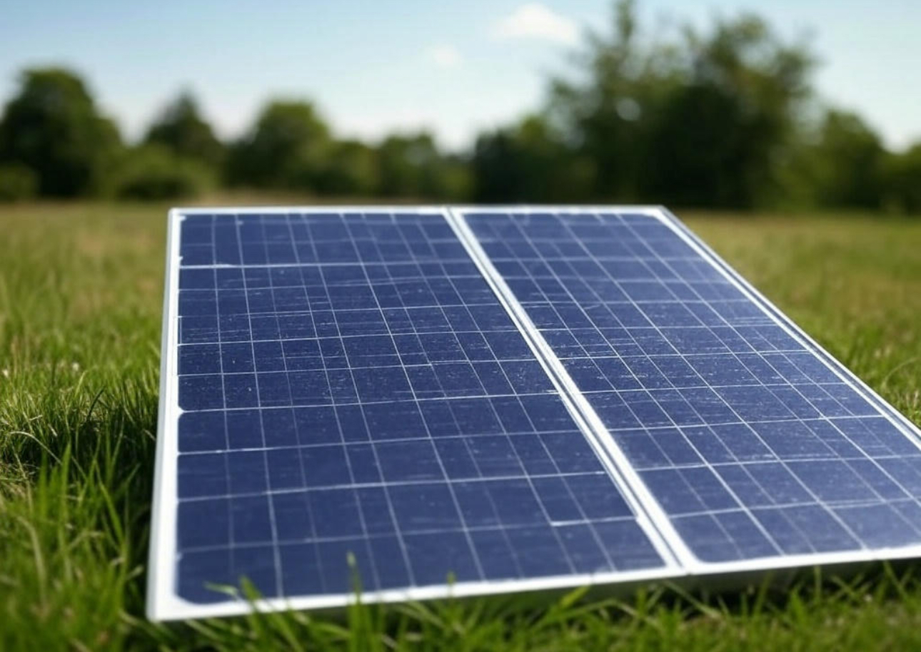
N-Type Wafers: Doped with phosphorus (P) or arsenic (As) for electron-based conductivity, preferred for high-speed digital ICs and solar cells.
1~100Ω Resistivity Range
Tailored resistivity ensures compatibility with diverse applications, from low-power sensors to high-current power devices.
Dust-Free Surface
Manufactured in cleanroom environments to minimize particulate contamination, critical for high-yield lithography and thin-film deposition.
Single-Sided Polishing
One side is mirror-polished for photolithography and device fabrication, while the unpolished side provides mechanical stability during handling.
Advantages of Single-Sided Polished & Dust-Free Design
Enhanced Process Control: The polished side ensures uniformity in photoresist coating and etching.
Reduced Defects: Dust-free surfaces minimize particle-induced failures during fabrication.
Cost Efficiency: Single-sided polishing lowers production costs while maintaining performance.
Versatility: Compatible with CVD, PVD, and epitaxial growth processes.
Why Choose 8-Inch Wafers?
Balanced Size: Offers a cost-effective middle ground between smaller (6-inch) and larger (12-inch) wafers.
Broad Compatibility: Widely used in legacy and emerging semiconductor tools.
High Yield: Optimized for medium-volume production with minimal material waste.
Conclusion
The 8-inch P/N Type 1~100Ω Dust-Free Single-Sided Polished Silicon Wafer is a versatile and reliable substrate for cutting-edge semiconductor applications. Its combination of precise doping, controlled resistivity, and pristine surface quality makes it indispensable for industries demanding high performance and process efficiency. Whether for power devices, MEMS, or optoelectronics, this wafer ensures robust performance in even the most demanding fabrication environments.