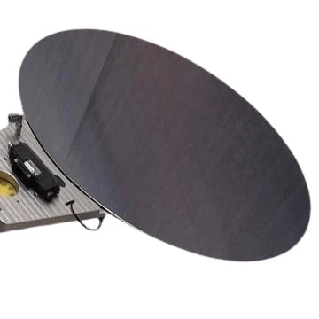
18-Inch Double-Sided Polished P-Type (100) Silicon Wafer (1–50Ω·cm) – Next-Gen Substrate for Advanced Semiconductor and Research Applications
Introduction
The 18-inch double-sided polished P-type (100) silicon wafer (1–50Ω·cm resistivity) represents a leap forward in semiconductor substrate technology. Engineered for next-generation applications, this ultra-large wafer combines exceptional surface uniformity, electrical precision, and scalability, making it ideal for advanced R&D, MEMS, and exploratory large-scale integration projects.
Key Features
18-Inch (450mm) Diameter:
Unparalleled Scalability: Increases die-per-wafer yield by over 2x compared to 12-inch wafers, reducing costs for high-volume R&D and pilot production.
Future-Ready Compatibility: Targets next-gen fabrication tools designed for 450mm processing, though currently optimized for specialized research systems.
P-Type (100) Crystal Orientation:
Uniform Atomic Structure: Ensures consistent epitaxial growth and oxide layer formation, critical for advanced CMOS, photovoltaics, and MEMS.
Thermal and Mechanical Stability: Withstands high-temperature processes (e.g., annealing, oxidation) and minimizes warping.
Double-Sided Polishing (DSP):
Ultra-Smooth Surfaces (Ra <0.2nm): Both sides are mirror-polished, enabling bidirectional processing for 3D ICs, MEMS, and photonic devices.
Defect-Free Fabrication: Reduces surface scattering and particle contamination in lithography and thin-film deposition.
Adjustable Resistivity (1–50Ω·cm):
Boron Doping Precision: Tailored for applications ranging from low-power logic devices (1–10Ω·cm) to high-voltage power components (20–50Ω·cm).
Technical Advantages
Surface Quality: DSP ensures Ra <0.2nm, critical for EUV lithography and atomic-layer deposition (ALD).
Material Purity: Low oxygen/carbon content (<5 ppba) via advanced Czochralski (CZ) growth.
Customization: Optional backside metallization (Al/Ti/Cu) or oxide/nitride layers for specialized workflows.
Technical Specifications
Type: P-type (Boron-doped)
Resistivity: 1–50Ω·cm (customizable)
Diameter: 18 inches (450mm)
Orientation: <100>
Thickness: 925±25µm (standard, customizable 700–1200µm)
Surface Finish: Double-sided polished (Ra <0.2nm)
TTV (Total Thickness Variation): <3µm
Why Choose This Wafer?
Pioneering Format: Addresses the industry’s roadmap for 450mm wafer adoption, bridging R&D and future production needs.
Research-Grade Precision: Complies with SEMI standards for resistivity uniformity (±3%) and particle control (<30/wafer, ≥0.1µm).
Technical Collaboration: Partner with suppliers offering co-development support for 450mm tool integration and process optimization.
Conclusion
The 18-inch double-sided polished P-type (100) silicon wafer (1–50Ω·cm) is a visionary substrate for pushing the boundaries of semiconductor innovation. While 450mm production remains nascent, this wafer empowers researchers and engineers to explore large-scale integration, novel device architectures, and next-gen MEMS/photonics. Its unmatched surface quality, scalability, and adaptability make it a cornerstone for tomorrow’s technologies.
Lead the future of semiconductor innovation – inquire about our 18-inch wafer solutions today!