High-Performance 12-Inch P-Type Double-Sided Polished Test Grade Silicon Wafer (1–100Ω·cm) – Ideal for Semiconductor Process Development & Equipment Calibration
Introduction
The 12-inch P-type double-sided polished Test Grade silicon wafer (1–100Ω·cm resistivity) is a cost-efficient, high-performance substrate tailored for non-production semiconductor applications. Engineered for process optimization, equipment calibration, and educational purposes, it combines precise resistivity control with superior surface quality, significantly reducing R&D costs while maintaining compatibility with industrial standards.
Key Features
12-Inch (300mm) Format:
Industrial Compatibility: Fully compatible with 300mm fabrication tools, including lithography scanners, etch systems, and CVD/PVD equipment.
Cost Efficiency: Optimized for small-batch R&D and academic use, offering substantial savings over production-grade wafers.
P-Type Doping (Boron):
Adjustable Resistivity (1–100Ω·cm): Supports a wide range of applications, from low-power logic devices to high-voltage component testing.
Controlled Electrical Properties: Ensures baseline performance for non-critical electrical validation, such as thin-film uniformity checks.
Double-Sided Polishing (DSP):
Ultra-Smooth Surfaces (Ra <0.5nm): Both sides are mirror-polished, enabling high-precision lithography alignment and uniform thin-film deposition.
Bidirectional Processing: Ideal for MEMS double-sided fabrication or advanced packaging technologies.
Test Grade Classification:
Non-Production Use: Designed for equipment calibration, process debugging, and training, avoiding waste of high-cost production wafers.
Controlled Defect Tolerance: Allows minor surface particles (<80 counts/wafer, ≥0.5μm) without compromising functional testing.
Technical Advantages vs. Production Wafers
| Feature | Production-Grade Wafers | Test Grade Wafers |
|---|---|---|
| Cost | High ($300+/wafer) | Low (150/wafer) |
| Surface Quality | Ultra-Precision (Ra <0.3nm) | High Precision (Ra <0.5nm) |
| Resistivity Control | Strict (±1%) | Moderate (±5%) |
| Defect Tolerance | Zero Defects Required | Controlled Defects Allowed |
| Lead Time | Long (6–8 weeks) | Short (48-hour shipping available) |
Technical Specifications
Type: P-type (Boron-doped)
Resistivity: 1–100Ω·cm (custom ranges available)
Diameter: 12 inches (300mm)
Orientation: <100> (standard)
Thickness: 775±25µm (customizable: 500–1000µm)
Surface Finish: Double-sided polished (Ra <0.5nm)
TTV (Total Thickness Variation): <5µm
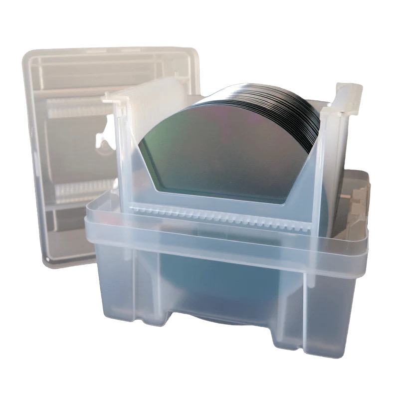
Packaging: Single-wafer or 25-wafer lots, anti-static vacuum-sealed
Why Choose This Wafer?
Cost Savings: Priced 60% lower than production-grade wafers, ideal for budget-sensitive projects.
Rapid Availability: In-stock solutions with 48-hour shipping to accelerate R&D timelines.
Quality Assurance: Guaranteed macro-defect-free surfaces (no cracks/chips) and >95% reflectivity (@633nm).
Customization: Optional backside metallization (Al/Cu) or localized patterning for specialized testing.
Conclusion
The 12-inch P-type double-sided polished Test Grade silicon wafer (1–100Ω·cm) delivers precision, affordability, and versatility for semiconductor process development, equipment calibration, and education. Its industrial compatibility and controlled performance make it indispensable for optimizing next-gen technologies, training engineers, or ensuring equipment reliability.
Contact us today to request samples and tailored solutions!