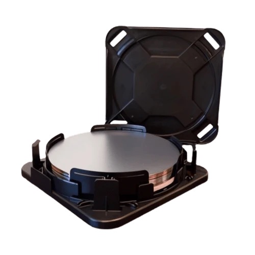
Economical and environmentally friendly 8 inch P/N Type (100) single-sided polished regeneration test wafer (1-100Ω·cm) - ideal for process development and equipment commissioning
introduction
The 8-inch P/N type (crystal direction <100>) regenerative test wafer (resistivity 1-100Ω·cm, single-side polished) is designed for non-volume production applications in the semiconductor industry, combining economy, environmental protection and functionality. By recovering and reprocessing high-purity silicon wafers, the substrate provides a cost-effective solution for process commissioning, equipment calibration and education, while reducing e-waste and driving sustainable development.
Core characteristic
Reclaimed Substrate Technology:
Environmental protection priority: Recovery of wafer fab test pieces or edge elimination pieces, after strict cleaning, polishing and recycling, reduce waste of resources.
Cost advantage: Price competitive production grade silicon chip reduced by more than 60%, suitable for budget sensitive research and development and teaching scenarios.
P/N type doping flexibility:
P-type (boron doped) and N-type (phosphorus/arsenic doped) optional: resistivity coverage 1-100Ω·cm, suitable for CMOS process development, ion implantation testing and other needs.
Basic electrical properties: meet the photolithographic alignment, film deposition uniformity verification and other non-precision electrical tests.
Single-Side Polish:
Polished surface (front Ra <1nm) : provides basic finish, compatible with photoresist coating, etching and CVD/PVD process testing.
Non-polished surface (back rough grinding treatment) : easy to grasp the mechanical arm, reduce equipment adaptation costs.
Dummy Grade positioning:
Non-mass production use: Specially used for equipment debugging, rough adjustment of process parameters and teaching demonstration to avoid waste of high-value mass production films.
Controlled defect tolerance: Allow minor surface particles (<100 PCS/piece, ≥0.5μm) and marginal micro-damage without affecting core function.
Typical application scenario
Equipment calibration and maintenance:
It is used to verify the alignment accuracy of lithography machine, test the rate of etching machine, monitor the uniformity of film deposition and other equipment debugging scenarios.
Initial process development test:
Validate new process parameters (such as annealing temperature, doping concentration) before volume to reduce trial and error costs.
University laboratory teaching:
Students can safely carry out photolithography, etching, cleaning and other basic technology practical operation, reduce the cost of teaching supplies.
Temporary vehicle and protective substrate:
As a temporary support in MEMS processes or advanced packaging to prevent contamination or mechanical damage to formal product pieces.
Advantages over mass production of silicon wafers
Characteristics Production grade silicon wafer regeneration test silicon wafer
High cost ($200+/ tablet) Very low (
50
-
50−80/ tablet)
Surface quality Ultra precision (Ra <0.5nm) Base grade (Ra <1nm)
Electrical parameter control is strict (resistivity ±1%) loose (resistivity ±10%)
Environmentally friendly (carbon footprint reduced by 40%+)
Long lead time (4-8 weeks) Short (standing stock, delivery within 72 hours)
Technical parameter
Type: P type (boron) /N type (Phosphorus/Arsenic) Optional
Resistivity: 1-100Ω·cm (segmented optional)
Diameter: 8 inches (200mm)
Crystal direction: <100>
Thickness: 725±25µm (500-800µm customizable)
Surface treatment: Single side polishing (front Ra <1nm), back sandblasting
Packing: 25 PCS/box, anti-static package
Choice reason
Plug and play compatibility: Suitable for mainstream 200mm devices such as ASML, TEL, and Lam Research, without hardware modification.
Strict quality control bottom line: Although it is Dummy Grade, it still ensures no macroscopic cracks and edge breakage, and the reflectivity of the polished surface is >90% (@633nm).
Green supply Chain support: Silicon Wafer Recycling Certification (R2v3/RIOS) is provided to help enterprises achieve ESG goals.
Flexible customization services: Support back metallization (Al/Ti), local graphics and other value-added processing to meet special test needs.
Conclusion
The 8-inch P/N type regenerative test wafer is an economical, environmentally friendly and functional trinity, making it a practical choice for semiconductor research and development, education and equipment maintenance. Whether it is accelerating the implementation of new processes, cultivating industry talent, or practicing green manufacturing, the substrate empowers every link in the semiconductor innovation chain with cost-effective and low-carbon properties.
Get samples now and experience a low-cost, efficient process validation solution!