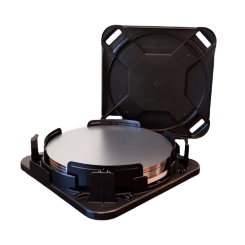
Economical 8-inch single-sided polished Dummy Grade wafers - ideal for semiconductor process testing and equipment calibration
introduction
The 8-inch single-sided polished Dummy Grade silicon chip is designed for semiconductor process development, equipment calibration and teaching experiment design. With economy and functionality as the core, it provides a cost-effective solution for non-mass production scenarios. Its compatibility with mainstream process equipment makes it an essential material for process commissioning in research and development laboratories, universities and fabs.
Core characteristic
Dummy Grade positioning:
Non-mass production use: Not used for final chip production, designed for equipment debugging, process verification and teaching experiment optimization, significantly reducing costs.
Surface quality control: single-side polishing (Ra <1nm), to meet the basic test requirements of lithography, film deposition and other processes.
8 inch (200mm) size:
Device compatibility: Suitable for mainstream 200mm wafer equipment, such as gluing machine, etching machine, CVD/PVD system, no additional modification is required.
Economy: Compared to 12-inch substrates, it is more suitable for small and medium-sized laboratory and educational institution budgets.
Single-side polishing process:
Polished surface (front) : Provides basic smoothness, supports photolithographic alignment and film uniformity testing.
Non-polished surface (back) : Retain the rough surface, easy to mechanical grasp or temporary fixing, reduce processing costs.
Flexible parameter configuration:
Thickness optional: 725±25µm (standard) or customized requirements.
Crystal direction optional: <100> (default), <111>, etc., suitable for different process development scenarios.
Technical parameter
Type: Dummy Grade Silicon (non-electronic grade)
Diameter: 8 inches (200mm)
Thickness: 725±25µm (500-800µm customizable)
Crystal direction: <100> (Default, <111> optional)
Surface treatment: single side polishing (front Ra <1nm), back sandblasting or rough grinding
Packing: Single piece or 25 pieces/box, ESD box package
Choice reason
Plug and play: Compatible with ASML, TEL, Applied Materials and other mainstream equipment, seamless access to existing production lines.
Strict quality control: Although it is Dummy Grade, it is still ensured that there are no macroscopic defects (cracks, pits) and the surface particle number is <50/ sheet (≥0.3µm).
Technical support: Provide process parameter recommendation and equipment adaptation report, shorten the commissioning cycle.
Conclusion
With the core values of "cost-effective, responsive and widely compatible", the 8-inch single-sided polished Dummy Grade silicon chip is an indispensable utility in semiconductor research and development, education and equipment maintenance. Whether it is optimizing new process parameters, training technical teams, or ensuring stable operation of equipment, the substrate enables your innovation process at low cost and high efficiency.
Contact us today to get a Dummy Grade wafer sample and start zero-risk process validation!