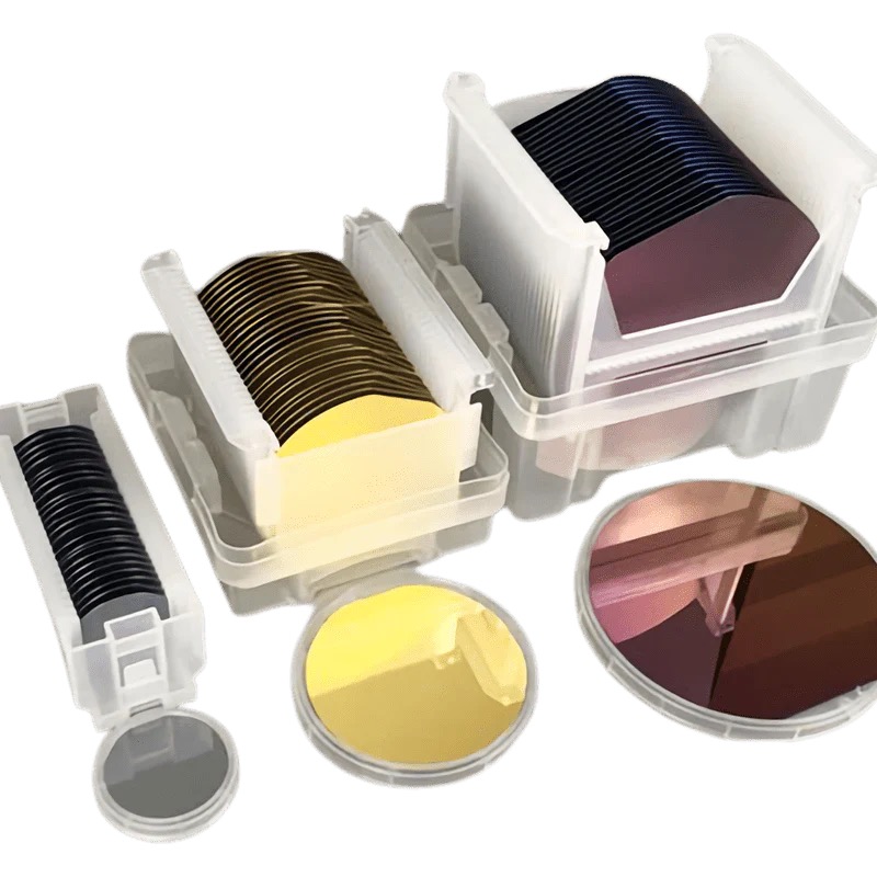
High-performance 12-inch P-type silicon substrates (1-100Ω·cm) with integrated aluminum/copper layers - the core solution for advanced power and high-frequency devices
introduction
12-inch P-type silicon substrates (1-100Ω·cm) with integrated aluminum (Al) or copper (Cu) metal layers are key materials for power electronics, radio frequency communications, and micro-electro-mechanical systems (MEMS) due to their large size economy, tunable electrical properties, and metal layer functionalization. It enables high electrical conductivity, thermal management and structural support through metal layers, enabling innovation in high-performance semiconductor devices.
Core characteristic
12-inch largeon economy: Compatible with 300mm wafer production line, reduce unit chip cost, meet advanced process requirements.
Uniformity control: resistivity (±5%), thickness (TTV <5µm) and metal layer uniformity e size
substrate:Mass productare strictly controlled to ensure yield.
P-type doping (boron doping) :
Resistivity range (1-100Ω·cm) : Support diverse needs from low-power logic devices (1-10Ω·cm) to high-power components (>50Ω·cm).
High carrier mobility: Reduces leakage current and improves device response speed and reliability.
Aluminum/Copper metal layer functionalization:
Advantages of aluminum layer:Low cost and high
compatibility: suitable for traditional sputtering/evaporation process, suitable for power device electrode and MEMS structure layer.
Oxidation resistance: A natural oxide layer (Al₂O₃) provides surface passivation for extended device life.
Advantages of copper layer:
Ultra-high conductivity: Resistivity as low as 1.7μΩ·cm, reducing interconnect resistance and improving RF device efficiency.
Excellent heat dissipation capacity: thermal conductivity ~400 W/m·K, to solve the thermal failure problem of high power density chips.
The thickness of the metal layer is adjustable: 0.1-5µm to meet the multiple needs of electrical conductivity, heat dissipation or mechanical support.
Surface treatment process:
Double-sided polishing (Ra <0.2nm) : provides atomically smooth surfaces for lithography and thin film deposition.
Selective metallization: Support graphical aluminum/copper layer deposition, direct integration of wire or heat dissipation structures.
Technological advantage
Multifunctional integration: Metal layer to achieve conductivity, heat dissipation, structural support "three in one", simplify the process steps.
Process flexibility: Support Al/Cu alone or combined deposition (such as Al-Cu alloys) to meet diverse design requirements.
High reliability: HTOL (high temperature service life) and TCT (temperature cycle) test, suitable for vehicle scale applications.
Cost optimization: The aluminum layer reduces material costs and the copper layer reduces etching losses through the Damascene process.
Technical parameter
Substrate Type: P-type silicon (boron-doped)
Resistivity: 1-100Ω·cm (segmented optional)
Diameter: 12 inches (300mm)
Crystal direction: <100> (standard, <111> can be customized)
Wafer thickness: 775±25µm
Metal layer options:
Aluminum layer (Al) : 0.1-3µm, purity >99.999%
Copper layer (Cu) : 0.1-5µm, plating/sputtering process is optional
Surface roughness (Ra) : <0.2nm (polished surface), <50nm (metallized surface)
Choice reason
Industrial-grade quality: SEMI compliant, JEDEC certified for reliability, supporting automotive electronics (AEC-Q100) applications.
Global Supply chain: Fast delivery of 12-inch wafers to customers in Asia, Europe and North America.
Technical support: Provide metal layer design rules (DRC) and thermal-electrical co-simulation models to accelerate customer product to market.
Conclusion
The 12-inch P-type silicon substrate (1-100Ω·cm) integrates aluminum/copper metal layers, making it a strategic material for power electronics, RF communications, and advanced packaging due to its large size economy, metal functional design, and excellent thermal performance. Whether it is improving the efficiency of 5G base stations, optimizing electric vehicle drive modules, or innovating MEMS sensor designs, the substrate breaks through with high performance and high reliability enabling technology.
Contact our technical team today to customize your metallized silicon substrate solution!