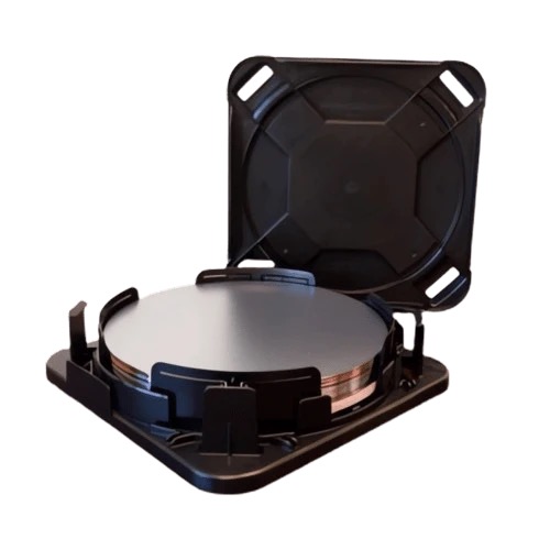
Eco-Friendly 12-Inch P-Type Reclaimed Silicon Wafer (1-100Ω·cm) with Double-Side Polishing for Sustainable Semiconductor Solutions
Introduction
The 12-inch P-type reclaimed silicon wafer with 1-100Ω·cm resistivity and double-side polishingis a sustainable and cost-effective solution for semiconductor research, development, and education. By repurposing high-quality silicon wafers, this substrate delivers excellent performance while reducing environmental impact. This article explores its features, applications, and advantages for eco-conscious semiconductor projects.
Key Features
Reclaimed Silicon Technology:
Eco-Friendly: Reduces waste by repurposing high-quality silicon wafers from previous manufacturing processes.
Cost-Effective: Provides a budget-friendly alternative to virgin wafers without compromising performance.
P-Type Doping (Boron):
Resistivity Range (1-100Ω·cm): Suitable for a wide range of applications, from low-power logic devices to high-power components.
High Carrier Lifetime: Ensures reliable performance with minimal leakage current.
Double-Side Polishing:
Ultra-Smooth Surfaces (Ra <0.3 nm): Both sides are mirror-polished, ideal for applications requiring bidirectional precision, such as MEMS and photonics.
Enhanced Uniformity: Ensures consistent thickness (TTV <5µm) and surface quality across the wafer.
12-Inch Diameter:
Scalability: Compatible with 300mm fabrication tools, supporting prototyping and small-scale production.
Versatility: Suitable for a wide range of semiconductor applications, from research to industrial use.
Advantages Over Virgin Wafers
Sustainability: Reduces silicon waste and promotes eco-friendly manufacturing practices.
Cost Savings: Offers a budget-friendly alternative for non-critical applications.
High Performance: Maintains excellent electrical and mechanical properties despite being reclaimed.
Flexibility: Suitable for a wide range of applications, from R&D to educational labs.
Technical Specifications
Type: P-type (Boron-doped)
Resistivity: 1-100Ω·cm (customizable)
Diameter: 12 inches (300mm)
Thickness: 775±25µm (standard)
Surface Finish: Double-side polished (Ra <0.3 nm)
TTV (Total Thickness Variation): <5µm
Why Choose This Wafer?
Eco-Conscious Manufacturing: Supports sustainable practices by reducing silicon waste.
Cost Efficiency: Provides high-quality wafers at a fraction of the cost of virgin substrates.
Quality Assurance: Rigorous inspection ensures reliable performance for non-critical applications.
Technical Support: Collaborate with suppliers offering expertise in reclaimed wafer integration.
Conclusion
The 12-inch P-type reclaimed silicon wafer with 1-100Ω·cm resistivity and double-side polishingis a sustainable and cost-effective solution for semiconductor research, education, and prototyping. Its eco-friendly manufacturing process, combined with excellent electrical and mechanical properties, makes it an ideal choice for labs and institutions aiming to reduce costs and environmental impact. Whether for MEMS development, educational purposes, or thin-film research, this wafer delivers the performance and versatility needed to support innovation.
Choose sustainable semiconductor solutions with this high-performance reclaimed wafer today!