High-Performance 8-Inch P-Type Silicon Wafer (1-100Ω·cm) with Aluminum Layer for Advanced Semiconductor Applications
ntroduction
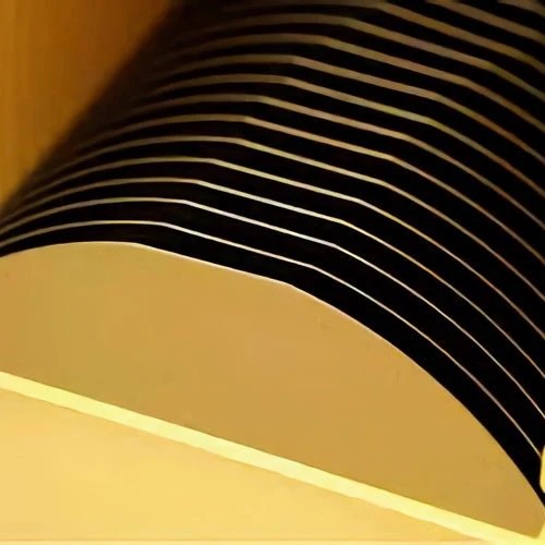
The 8-inch P-type silicon wafer with 1-100Ω·cm resistivity and an integrated aluminum layer is a versatile and high-performance substrate designed for advanced semiconductor applications. Combining the electrical properties of P-type silicon with the thermal and conductive benefits of aluminum, this wafer is ideal for power electronics, MEMS, and optoelectronic devices. This article explores its features, applications, and advantages in modern technology.
Key Features
8-Inch Diameter:
Scalability: Compatible with 200mm fabrication tools, enabling cost-effective mid- to high-volume production.
Uniformity: Advanced manufacturing ensures consistent thickness (TTV <5µm) and resistivity across the wafer.
P-Type Doping (Boron):
Resistivity Range (1-100Ω·cm): Tailored for applications requiring precise hole conduction, from low-power logic devices to high-power components.
High Carrier Lifetime: Reduces leakage current and enhances device reliability.
Integrated Aluminum Layer:
Enhanced Conductivity: Provides excellent electrical and thermal conductivity, ideal for power devices and heat dissipation.
Mechanical Stability: Improves wafer strength and durability during processing and operation.
Surface Passivation: Protects the silicon surface from oxidation and contamination.
Surface Finish Options:
Single-Side Polishing: Mirror-polished frontside (Ra <0.5 nm) for smooth device fabrication; backside aluminum layer for conductivity.
Double-Side Polishing: Ultra-smooth surfaces on both sides for applications requiring bidirectional precision.
Advantages Over Conventional Substrates
Enhanced Thermal Management: Aluminum layer improves heat dissipation, critical for high-power applications.
Improved Electrical Conductivity: Reduces energy loss and enhances device performance.
Mechanical Durability: Aluminum layer adds strength, reducing wafer warping and breakage.
Customization: Adjust resistivity, aluminum layer thickness, and surface finish for specific needs.
Technical Specifications
Type: P-type (Boron-doped)
Resistivity: 1-100Ω·cm (customizable)
Diameter: 8 inches (200mm)
Thickness: 725±25µm (standard)
Aluminum Layer Thickness: 0.5-5µm (customizable)
Surface Finish: Single/double-side polished (Ra <0.5 nm)
TTV (Total Thickness Variation): <5µm
Why Choose This Wafer?
Industry Compliance: Meets SEMI standards for resistivity uniformity, flatness, and surface cleanliness.
Quality Assurance: Rigorous defect inspection ensures high yields in demanding fabrication processes.
Technical Support: Collaborate with suppliers for doping optimization and aluminum layer integration.
Conclusion
The 8-inch P-type silicon wafer with 1-100Ω·cm resistivity and an integrated aluminum layer is a game-changer for advanced semiconductor applications. Its combination of electrical performance, thermal management, and mechanical durability makes it indispensable for power electronics, MEMS, and optoelectronics. Whether scaling prototypes or optimizing high-volume production, this wafer delivers the precision, reliability, and versatility needed to drive technological advancements.
Upgrade your semiconductor projects with this high-performance, customizable substrate today!