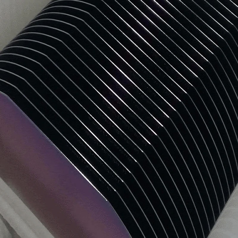
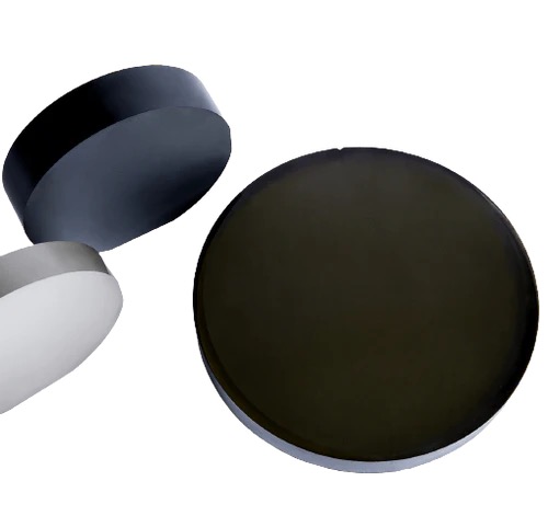
High-performance 12-inch P-type silicon wafers (1-100Ω·cm) with integrated silicon nitride (SiN) layers - the ideal substrate for advanced semiconductor manufacturing
introduction
The 12-inch P-type silicon wafer (resistivity 1-100Ω·cm) combined with the silicon nitride (SiN) layer is the versatile, high-performance core substrate in the modern semiconductor industry. Its optimized electrical properties and chemical stability of the SiN layer make it important in the field of integrated circuits, power electronics and sensors. This paper describes its core features, application scenarios and technical advantages in detail.
Core characteristic
12 "large size advantages:
High mass production efficiency: compatible with mainstream semiconductor production lines, reduce unit chip costs, and improve manufacturing economic benefits.
Uniformity control: Advanced wafer fabrication technology ensures consistency in resistivity, thickness, and SiN layer (TTV <5µm).
P-type doping (boron doping) :
Adjustable resistivity (1-100Ω·cm) : Supports diverse needs from low-power logic devices to high-power components.
High carrier lifetime: Reduces leakage current and improves device reliability.
Silicon nitride (SiN) functional layer:
Chemical passivation and insulation: prevent surface oxidation and contamination, reduce interface defect density, and improve the long-term stability of the device.
Optical and mechanical properties: High refractive index and scratch resistance for protection of optoelectronic devices and MEMS structures.
Thermal stability: Withstand high temperature processes (such as annealing, diffusion), compatible with subsequent process integration.
Surface treatment process:
Double or single side polishing +SiN deposition: ** Flexible choice according to application requirements, optimising cost and performance balance.
Technological advantage
Multi-functional integration: The SiN layer achieves the "trinity" of passivation, insulation and optical regulation, simplifying the process steps.
High reliability: Resistance to moisture and corrosion, extending the service life of the device in harsh environments such as automotive electronics.
Process compatibility: Support various SiN deposition technologies such as LPCVD/PECVD, suitable for existing production line equipment.
Customized services: The resistivity (1-100Ω·cm), SiN layer thickness (50-500nm) and crystal direction (<100>/<111>) can be customized.
Technical parameter
Type: P-type silicon (boron doped)
Resistivity: 1-100Ω·cm (segmented optional)
Diameter: 12 inches (300mm)
Crystal direction: <100> (standard, others can be customized)
Wafer thickness: 775±25µm
SiN layer Thickness: 50-500nm (customizable)
Surface treatment: double-sided polishing or single-side polishing +SiN deposition
TTV (total thickness deviation) : <5µm
Choice reason
Industrial-grade quality: SEMI compliant and ISO certified to ensure batch stability and traceability.
Global supply chain support: Fast delivery of 12-inch wafers to customers in North America, Asia and Europe.
Technical collaboration: Provide SiN layer process parameter optimization solutions to help customers improve device performance.
Conclusion
12-inch P-type silicon wafers (1-100Ω·cm) with integrated silicon nitride (SiN) layers are a strategic material for semiconductor manufacturing due to their large size economy, tunable electrical properties, and versatile passivation capabilities. Whether advancing advanced processes, optimizing power devices, or innovating MEMS designs, the substrate enables technological breakthroughs with superior performance.
Contact us today for a customized silicon wafer solution and lead the semiconductor innovation wave!