2-Inch N-Type Gallium Nitride (GaN) Dummy Grade Wafer: Cost-Effective Solutions for Semiconductor Testing and R&D
Introduction
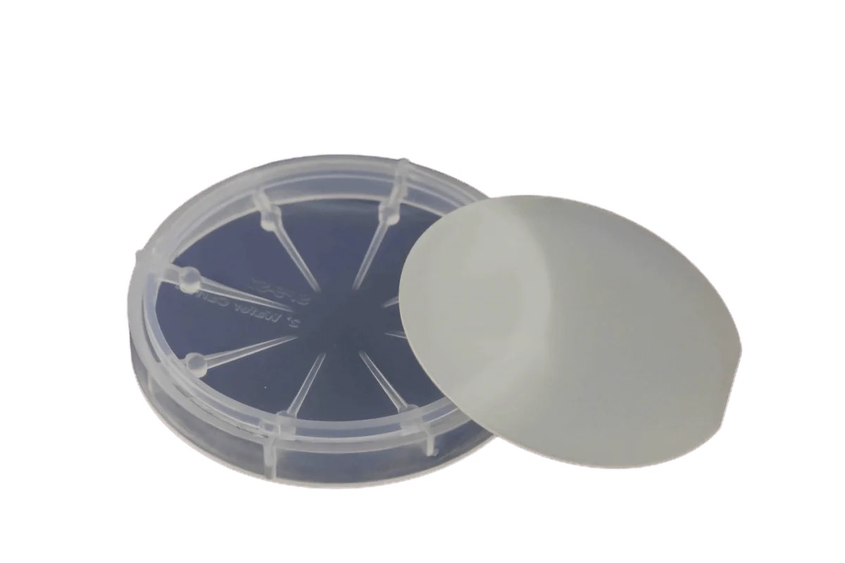
The 2-inch N-Type Gallium Nitride (GaN) Dummy Grade Wafer is a specialized substrate designed for semiconductor process development, equipment calibration, and non-production testing. Unlike prime-grade wafers, dummy-grade substrates prioritize cost efficiency over ultra-low defect density, making them ideal for iterative R&D cycles and fab tool validation. With controlled N-type doping and standardized specifications, this wafer streamlines prototyping for applications like 5G RF devices, power converters, and optoelectronics17.
Key Features and Specifications
Material Properties
GaN Advantages: Wide bandgap (3.4 eV), high thermal conductivity (2.3 W/cm·K), and breakdown voltage (>1,000 V), enabling high-temperature and high-frequency operation16.
N-Type Doping: Achieved via silicon (Si) or germanium (Ge), providing resistivity ≤0.05 Ω·cm for low-resistance conductive layers1.
Dummy Grade Specifications
Defect Tolerance: Higher allowable defect density (e.g., micro-pipes, surface scratches) compared to production-grade wafers, reducing costs for non-critical applications6.
Surface Finish: Single-side polished (Ra ≤0.3 nm) for lithography compatibility, with etched or lapped backside for mechanical stability1.
Standard Dimensions:
Diameter: 50.8±0.3 mm (2-inch)
Thickness: 400±30 μm
Orientation: (0001) Ga-face with controlled off-cut angles1.
Customization Options
Available in thicknesses from 0.1–1.0 mm and tailored surface roughness (slicing/lapping) for specific tool calibration needs1.
Applications in Semiconductor Workflows
Process Development
Used to optimize epitaxial growth (e.g., GaN-on-SiC or GaN-on-sapphire) and validate deposition/etching parameters without wasting prime-grade materials27.
Equipment Calibration
Ensures alignment and uniformity in lithography, CVD, and ion implantation tools, critical for maintaining yield in high-volume production1.
Educational and Academic Research
Enables affordable experimentation in university labs for studies on GaN material properties, defect analysis, and device physics6.
Prototyping for Power Electronics
Tests high-voltage MOSFETs and HEMTs (High-Electron-Mobility Transistors) for EV chargers and renewable energy systems26.
5G RF Testing
Validates performance of RF amplifiers and mmWave components in 5G base stations and satellite communication systems1.
Advantages of Dummy Grade GaN Wafers
Cost Efficiency
Priced significantly lower than prime-grade wafers, ideal for budget-constrained projects1.
Risk Mitigation
Reduces financial losses during high-risk process iterations (e.g., novel etch chemistries or doping profiles)7.
Scalability
Compatible with both legacy 2-inch tools and advanced 4-inch/6-inch production lines, easing technology transitions6.
Market Trends and Supplier Landscape
Growing Demand in China
Chinese manufacturers like JXT and Homray Material dominate GaN substrate production, offering customized dummy-grade wafers with rapid turnaround17.
Focus on 5G and Green Energy
Rising investments in 5G infrastructure and EVs drive demand for GaN testing wafers to accelerate device commercialization26.
Technological Innovations
Advances in HVPE (Hydride Vapor Phase Epitaxy) and MOCVD (Metal-Organic Chemical Vapor Deposition) improve defect control even in dummy-grade substrates1.
Why Choose 2-Inch N-Type GaN Dummy Wafers?
R&D Flexibility: Enables rapid iteration of novel device architectures (e.g., vertical GaN transistors)6.
Compatibility: Works with standard semiconductor fabrication tools, avoiding costly equipment upgrades1.
Sustainability: Reduces material waste by repurposing test wafers for multiple process cycles7.
Conclusion
The 2-inch N-Type GaN Dummy Grade Wafer is an indispensable tool for semiconductor innovation, bridging the gap between research and mass production. Its cost-effectiveness, coupled with GaN’s inherent performance advantages, makes it critical for advancing technologies in 5G, electric vehicles, and renewable energy. For tailored specifications or bulk orders, collaborate with leading suppliers like JXT or Homray Material, which offer comprehensive technical support and global logistics17.