2-Inch N-Type Gallium Nitride (GaN) P Grade Wafer: Compact Powerhouse for Cutting-Edge Semiconductor Innovation
Introduction
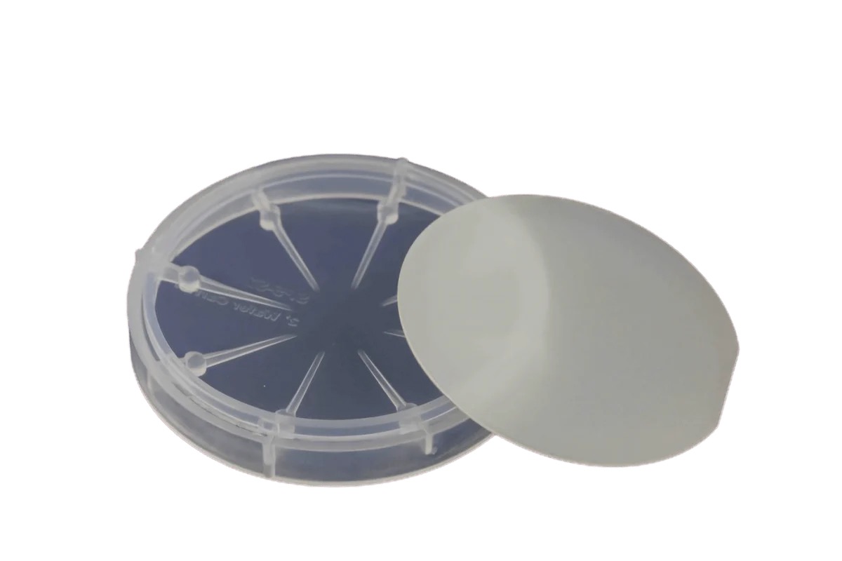
The 2-inch N-Type Gallium Nitride (GaN) P Grade Wafer is a compact yet powerful semiconductor substrate designed for cutting-edge research and niche applications. Combining GaN’s exceptional wide-bandgap properties with N-type doping and low defect density, this wafer is ideal for prototyping high-frequency, high-power, and optoelectronic devices. Its smaller size offers cost efficiency and flexibility, making it indispensable for academic labs, startups, and specialized industrial projects.
Key Features
Material Excellence
Gallium Nitride (GaN): A wide-bandgap semiconductor (3.4 eV) enabling superior thermal stability, high breakdown voltage (>1,000 V), and efficiency at high frequencies.
N-Type Doping: Achieved via silicon (Si) or germanium (Ge), providing high electron mobility (~2,000 cm²/Vs) for low-resistance conductive channels.
P Grade Quality
Ultra-Low Defect Density: < 10⁶ cm⁻² dislocation density, critical for reliable high-electron-mobility transistors (HEMTs) and laser diodes.
Uniform Crystal Structure: Grown via hydride vapor phase epitaxy (HVPE) or metal-organic chemical vapor deposition (MOCVD), ensuring consistent electrical performance.
2-Inch Diameter
Optimized for R&D flexibility, reducing material costs and enabling rapid iteration in device prototyping.
Compatible with legacy equipment, avoiding the need for expensive fab upgrades.
Surface Precision
Single-side polished (Ra < 0.2 nm) for nanoscale lithography and high-quality epitaxial layer growth.
Applications
High-Frequency RF Devices
5G and mmWave Technology: Supports RF power amplifiers and low-noise amplifiers (LNAs) for next-gen communication systems.
Satellite Communications: Enhances signal integrity in compact, high-efficiency transceivers.
Power Electronics
Fast Chargers: Enables ultra-efficient DC-DC converters for EVs and consumer electronics.
Renewable Energy Systems: Used in solar inverters and grid storage solutions for minimal energy loss.
Optoelectronics
UV-C LEDs: Critical for portable sterilization devices and water purification systems.
Blue Laser Diodes: Powers LiDAR sensors for autonomous vehicles and precision medical tools.
Defense and Aerospace
Radiation-resistant GaN components for satellite power systems and high-frequency radar arrays.
Manufacturing and Quality Assurance
Advanced Growth Techniques
HVPE: Produces thick, low-defect GaN layers for vertical power devices.
MOCVD: Enables precise doping control for HEMTs and multi-quantum well structures.
Defect Control
Chemical-mechanical polishing (CMP) and plasma etching minimize surface defects.
In-situ monitoring ensures doping uniformity (±3%) and resistivity stability (0.01–0.1 Ω·cm).
Rigorous Testing
X-ray Topography (XRT): Maps crystal defects and strain distribution.
Hall Effect Measurements: Verifies carrier concentration and mobility.
Market Trends
R&D Focus
The 2-inch GaN wafer market thrives in academic and industrial labs, driven by demand for novel device architectures like quantum sensors and terahertz emitters.
China’s semiconductor sector is investing in domestic GaN production, with firms like Enkris Semiconductor advancing 4-inch and 6-inch wafer technologies.
Miniaturization Wave
Compact 2-inch wafers align with trends in IoT, wearables, and portable electronics requiring small-footprint, high-efficiency components.
Sustainability Edge
GaN’s energy-saving capabilities support global decarbonization goals, reducing power losses in converters by up to 60% compared to silicon.
Why Choose 2-Inch N-Type GaN P Grade Wafers?
Cost-Effective R&D: Lower upfront investment for prototyping vs. larger wafer sizes.
High Precision: P Grade quality ensures reproducibility in sensitive experiments.
Scalability: Seamless transition to 4-inch or 6-inch wafers for mass production.
Future-Ready: Ideal for exploring emerging fields like GaN-based quantum computing and photonic integrated circuits.
Conclusion
The 2-inch N-Type Gallium Nitride P Grade Wafer is a vital tool for advancing semiconductor innovation, bridging the gap between theoretical research and commercial deployment. Its unparalleled performance in high-frequency, high-power, and optoelectronic applications positions it at the forefront of technologies shaping 6G, green energy, and smart healthcare.