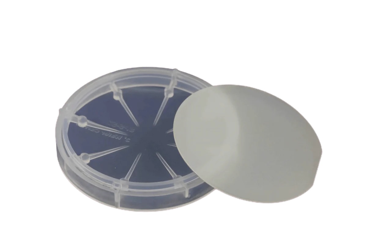
4-Inch N-Type Gallium Nitride (GaN) P Grade Wafer: High-Performance Substrate for Advanced Semiconductor Devices
Introduction
The 4-inch N-Type Gallium Nitride (GaN) P Grade Wafer represents a cutting-edge advancement in semiconductor materials, designed to meet the demands of next-generation high-frequency and high-power applications. With superior electron mobility, thermal stability, and breakdown voltage, GaN substrates are revolutionizing industries such as 5G communications, electric vehicles, and renewable energy systems.
Key Features of the 4-Inch N-Type GaN P Grade Wafer
Material Superiority
Gallium Nitride (GaN): A wide-bandgap semiconductor (3.4 eV) enabling high-temperature operation and efficiency in high-voltage environments.
N-Type Doping: Achieved via silicon (Si) or germanium (Ge) doping, providing high electron concentration (10¹⁷–10¹⁹ cm⁻³) for low-resistance conductive channels.
P Grade Quality
Low Defect Density: < 10⁶ cm⁻² dislocation density, ensuring reliability for high-performance devices like HEMTs and laser diodes.
Uniform Crystal Growth: Produced via hydride vapor phase epitaxy (HVPE) or metal-organic chemical vapor deposition (MOCVD), guaranteeing consistent electrical and structural properties.
4-Inch Diameter
Balances cost-efficiency and scalability for R&D and pilot production, bridging the gap between smaller R&D wafers and mass-production 6-inch/8-inch formats.
Surface Finish
Single-side polished (Ra < 0.2 nm) for precise lithography and epitaxial layer deposition.
Applications in Advanced Semiconductor Devices
5G and RF Communication
RF Power Amplifiers: GaN’s high electron saturation velocity (2.5×10⁷ cm/s) supports millimeter-wave (mmWave) 5G base stations and radar systems.
Low-Noise Amplifiers (LNAs): Enhances signal clarity in satellite and wireless communication.
Power Electronics
High-Efficiency Converters: Used in EV fast chargers and data center power supplies, reducing energy losses by up to 50% compared to silicon-based devices.
Ultra-Fast Switches: Enables MHz-range switching in renewable energy inverters and industrial motor drives.
Optoelectronics
Laser Diodes: Blue and UV lasers for LiDAR, optical storage, and medical equipment.
UV LEDs: Critical for water purification and sterilization systems.
Defense and Aerospace
Radiation-hardened GaN devices for satellite communications and high-power radar systems.
Manufacturing and Quality Control
Crystal Growth Techniques
HVPE Method: Produces thick, low-defect GaN layers for high-voltage vertical devices.
MOCVD Process: Enables precise doping and multi-layer epitaxial structures for HEMTs.
Defect Mitigation
Advanced etching and polishing techniques minimize threading dislocations and surface pits.
In-situ monitoring systems ensure doping uniformity (±5%) and resistivity control (0.01–0.1 Ω·cm).
Wafer Characterization
X-ray Diffraction (XRD): Validates crystal orientation and strain.
Photoluminescence (PL): Assesses optical quality and defect distribution.
Market Trends and Competitive Advantages
Growing Demand
The global GaN power device market is projected to exceed $2 billion by 2027, driven by EV adoption and 5G rollout.
China’s semiconductor initiatives prioritize GaN R&D, with companies like Enkris Semiconductor leading in 6-inch wafer production.
Technical Innovations
Vertical GaN Devices: Emerging for ultra-high-voltage (>1,200 V) applications, reducing reliance on silicon carbide (SiC).
GaN-on-Silicon: Lowers costs for consumer electronics but faces competition from native GaN substrates in high-end markets.
Sustainability Benefits
GaN’s high efficiency reduces energy waste, aligning with global carbon-neutral goals.
Why Choose 4-Inch N-Type GaN P Grade Wafers?
R&D Flexibility: Ideal for prototyping novel device architectures without the high cost of larger wafers.
Performance Consistency: P Grade quality ensures repeatable results in demanding applications.
Future-Proofing: Compatible with both current RF/power technologies and emerging quantum devices.
Conclusion
The 4-inch N-Type Gallium Nitride P Grade Wafer is a cornerstone of next-generation semiconductor innovation, offering unmatched performance in high-frequency, high-power, and optoelectronic applications. As industries transition to energy-efficient and high-speed technologies, GaN substrates will play a pivotal role in enabling breakthroughs from 6G networks to smart grids.