Aluminum Nitride Wafer 1-2 Inch AIN Mono High Purity Semiconductor Substrate: Powering Next-Gen Electronics
Introduction
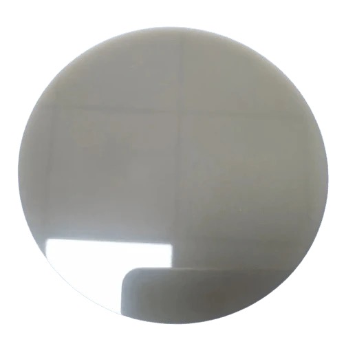
Aluminum Nitride (AIN) wafers are emerging as critical materials in high-performance electronics, offering a unique combination of thermal conductivity, electrical insulation, and compatibility with cutting-edge semiconductor processes. The 1-2 inch AIN monocrystalline high-purity substratestands out for its ability to address thermal and high-frequency challenges in modern devices, from 5G infrastructure to power electronics. This article delves into its properties, manufacturing processes, and transformative applications.
Key Properties of AIN Monocrystalline Substrates
Exceptional Thermal Conductivity (170–200 W/m·K):
Surpasses alumina and silicon, enabling efficient heat dissipation in high-power devices like LEDs and laser diodes.
Electrical Insulation:
High resistivity (>10¹⁴ Ω·cm) prevents current leakage, ideal for RF and microwave circuits.
Crystal Structure & Compatibility:
Hexagonal wafers with a lattice structure closely matched to gallium nitride (GaN), facilitating high-quality epitaxial growth for optoelectronic devices.
High Purity (>99.999%):
Minimizes defects and impurities, critical for reliability in semiconductor manufacturing.
Manufacturing Process & Challenges
Crystal Growth Techniques:
Physical Vapor Transport (PVT): Dominates AIN monocrystalline growth, requiring temperatures >2,000°C in a nitrogen-rich environment.
Chemical Vapor Deposition (CVD): Used for thin-film applications but less common for bulk substrates.
Surface Polishing:
Precision polishing achieves sub-nanometer surface roughness (<0.2 nm Ra), essential for epitaxial processes.
Scalability Challenges:
Producing large-diameter wafers (>2 inches) remains difficult due to AIN’s brittleness and high melting point.
Applications in Advanced Technologies
RF & 5G Communications:
AIN substrates enable low-loss, high-frequency GaN amplifiers for 5G base stations and satellite systems.
Power Electronics:
Used in high-voltage devices (e.g., MOSFETs, HEMTs) for EVs and renewable energy inverters, reducing thermal bottlenecks.
Optoelectronics:
Base material for UV LEDs, laser diodes, and sensors, leveraging AIN’s wide bandgap (6.2 eV).
MEMS & Sensors:
Supports resonant sensors and piezoelectric devices due to its acoustic wave properties.
Advantages Over Competing Materials
Thermal Performance: Outperforms silicon carbide (SiC) and alumina in thermal management.
GaN Compatibility: Superior lattice match to GaN compared to sapphire or silicon, reducing defects in epitaxial layers.
Durability: Resists chemical corrosion and thermal shock, suitable for harsh environments.
Market Trends & Future Outlook
5G and IoT Expansion:
The global RF semiconductor market is projected to reach $46B by 2027, driven by AIN/GaN devices.
EV and Renewable Energy Growth:
Demand for efficient power modules fuels AIN adoption in automotive and solar industries.
Research Innovations:
Focus on scaling wafer sizes (3-4 inches) and reducing production costs via hybrid AIN-on-SiC/Si solutions.
Conclusion
The 1-2 inch Aluminum Nitride monocrystalline high-purity substrate is a cornerstone of next-generation electronics, bridging the gap between thermal management, high-frequency performance, and semiconductor innovation. While manufacturing challenges persist, advancements in crystal growth and polishing technologies are paving the way for broader adoption. As industries push toward miniaturization and higher efficiency, AIN wafers will remain indispensable in powering 5G, EVs, and beyond.