Diamond Wafer Orientation (100) Double-Side Polished Semiconductor Substrate: Pioneering High-Performance Electronics
Introduction
Diamond, renowned as the "ultimate semiconductor," is revolutionizing high-performance electronics with its exceptional thermal, electrical, and mechanical properties. The Diamond Wafer Orientation (100) Double-Side Polished Semiconductor Substrate represents a breakthrough in material science, combining the advantages of (100) crystal orientation and ultra-smooth surfaces. This article explores its technical specifications, applications, and transformative potential in next-generation technologies like high-power electronics, quantum computing, and RF devices.
Key Features of Diamond Wafer (100) Double-Side Polished Substrate
Crystal Orientation (100):
Enhanced Carrier Mobility: The (100) orientation optimizes electron and hole mobility, critical for high-speed semiconductor devices.
Uniform Epitaxial Growth: Provides a consistent lattice structure for depositing GaN, AlN, or diamond thin films.
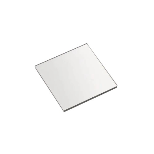
Double-Side Polished Precision:
Surface Roughness <0.1 nm Ra: Ultra-smooth surfaces minimize scattering losses in optical and RF applications.
Parallelism <1 µm: Ensures uniformity for advanced lithography and bonding processes.
Unrivaled Thermal Conductivity:
2,200 W/m·K: Dissipates heat 5x faster than copper, preventing thermal throttling in high-power devices.
Chemical and Mechanical Resilience:
Resists acids, plasmas, and physical wear, ideal for harsh environments like aerospace and industrial systems.
Wide Bandgap (5.5 eV):
Supports operation at extreme voltages (>10 kV) and temperatures (>500°C).
Applications in Advanced Technologies
High-Power Electronics:
EV and Renewable Energy: Diamond-based power devices (e.g., MOSFETs, Schottky diodes) reduce energy loss in 800V EV inverters and solar converters.
5G and RF Amplifiers: Low-loss diamond substrates enable high-frequency GaN amplifiers for 6G and satellite communication.
Quantum Computing:
Hosts nitrogen-vacancy (NV) centers for qubit arrays, leveraging diamond’s quantum coherence at room temperature.
Thermal Management:
Heat spreaders for high-density AI chips and laser diodes, preventing performance degradation.
Optoelectronics:
UV sensors and laser windows benefit from diamond’s transparency and durability.
Production Challenges & Innovations
Crystal Growth:
Challenge: Growing large, defect-free single-crystal diamond via CVD (Chemical Vapor Deposition) is slow and costly.
Solution: Microwave plasma CVD with methane/hydrogen gas mixtures, optimized for (100) orientation.
Polishing Technology:
Challenge: Diamond’s hardness (10 Mohs) complicates polishing.
Solution: Mechanical-chemical polishing (MCP) with diamond slurry and iron-based plates.
Cost Efficiency:
Challenge: High production costs limit adoption.
Solution: Heterogeneous integration (e.g., diamond-on-SiC) to reduce substrate size requirements.
Market Trends and Future Outlook
High-Power Demand:
The diamond semiconductor market is projected to grow at 25% CAGR (2023–2030), driven by EV and renewable energy sectors.
Quantum Leap:
Quantum computing investments (e.g., U.S. National Quantum Initiative) prioritize diamond for scalable qubit architectures.
Defense and Aerospace:
Radar and hypersonic systems adopt diamond substrates for thermal resilience in extreme conditions.
Conclusion
The Diamond Wafer Orientation (100) Double-Side Polished Substrate is redefining the boundaries of semiconductor technology. Its unmatched thermal conductivity, electrical performance, and surface precision make it indispensable for high-power electronics, quantum systems, and cutting-edge RF applications. While production challenges persist, advancements in CVD growth and polishing techniques are paving the way for cost-effective scalability. As industries push toward higher efficiency and miniaturization, diamond substrates will play a pivotal role in shaping the future of electronics.