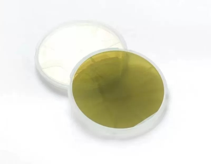
Silicon Carbide Substrate 6-Inch & 8-Inch NG Grade N-Type 4H-SiC Wafer for IGBT: Cost-Effective Solutions for Power Electronics
Introduction
As the demand for high-efficiency power electronics surges, Silicon Carbide (SiC) substrates remain critical for advancing Insulated Gate Bipolar Transistors (IGBTs). The 6-inch and 8-inch NG Grade N-Type 4H-SiC wafers offer a cost-effective solution for R&D, process calibration, and prototyping. While not meeting full production-grade standards, these substrates enable manufacturers to refine processes, reduce waste, and accelerate innovation in electric vehicles (EVs), renewable energy, and industrial systems. This article explores their technical attributes, applications, and role in driving the next generation of power electronics.
Key Features of NG Grade N-Type 4H-SiC Wafers
Material Specifications
4H-SiC Polytype: High electron mobility (900 cm²/Vs) and thermal conductivity (490 W/m·K) support high-frequency, high-temperature IGBT operation.
N-Type Doping: Nitrogen-doped for carrier densities of 1e18–1e19 cm⁻³, optimized for voltage tolerance up to 3.3kV.
NG Grade Utility
Cost Efficiency: Lower-cost alternative to production-grade wafers for equipment calibration, process testing, and pilot runs.
Defect Tolerance: Accepts minor crystal imperfections (e.g., micropipes, stacking faults) unsuitable for commercial devices but ideal for R&D.
Scalability
6-inch (150mm) & 8-inch (200mm) Sizes: Larger diameters improve economies of scale, with 8-inch wafers offering 56% more dies than 6-inch.
Applications in IGBT Development
EV Power Inverters
Prototype SiC IGBTs for 800V charging systems, enhancing efficiency by 10–15% compared to silicon-based solutions.
Renewable Energy Systems
Test high-voltage SiC IGBT modules for solar inverters and wind turbine converters, reducing energy losses.
Industrial Motor Drives
Validate high-frequency switching performance in automation and data center power supplies.
5G Infrastructure
Develop GaN-on-SiC RF devices for low-loss 5G base stations using semi-insulating SiC variants.
Role of NG Grade Wafers in Manufacturing
Process Calibration
Optimize epitaxial growth (CVD) and lithography parameters without wasting high-cost production-grade substrates.
Equipment Testing
Validate diamond wire saws, plasma etchers, and polishing tools for 6-inch/8-inch compatibility.
Yield Improvement
Identify defect patterns and refine defect-mitigation strategies in pilot production phases.
Production Challenges & Solutions
Crystal Growth Defects
Challenge: NG Grade wafers may exhibit micropipes or basal plane dislocations (BPDs).
Solution: AI-driven PVT (Physical Vapor Transport) optimization to reduce defect propagation.
Doping Uniformity
Challenge: Inconsistent nitrogen distribution in large-diameter wafers.
Solution: Multi-zone CVD reactors with real-time gas flow monitoring.
Cost Management
Challenge: High capital investment for 8-inch SiC production lines.
Solution: Leverage NG Grade wafers to minimize R&D costs and de-risk scaling efforts.
Market Trends & Innovations
EV Market Expansion
SiC demand for EVs is projected to grow at a 30% CAGR (2023–2030), driven by 800V architectures.
8-Inch Wafer Adoption
Industry leaders like Wolfspeed and STMicroelectronics aim to reduce SiC costs by 40% through 8-inch scaling by 2027.
Hybrid Technologies
SiC/Si hybrid IGBT modules combine cost efficiency and performance for consumer electronics and smart grids.
Conclusion
The 6-inch and 8-inch NG Grade N-Type 4H-SiC wafers are indispensable for advancing IGBT technology, offering a balance between performance and affordability. By enabling cost-effective R&D and process optimization, these substrates accelerate the adoption of SiC in EVs, renewables, and industrial systems. As manufacturers refine defect control and scale production, NG Grade wafers will play a pivotal role in achieving the cost targets needed for widespread SiC adoption.