Silicon Carbide Substrate 6-Inch 4H N-Type Production/Dummy Grade SiC Wafer for IGBT: Driving Efficiency in Power Electronics
Introduction to SiC Substrates and IGBTs
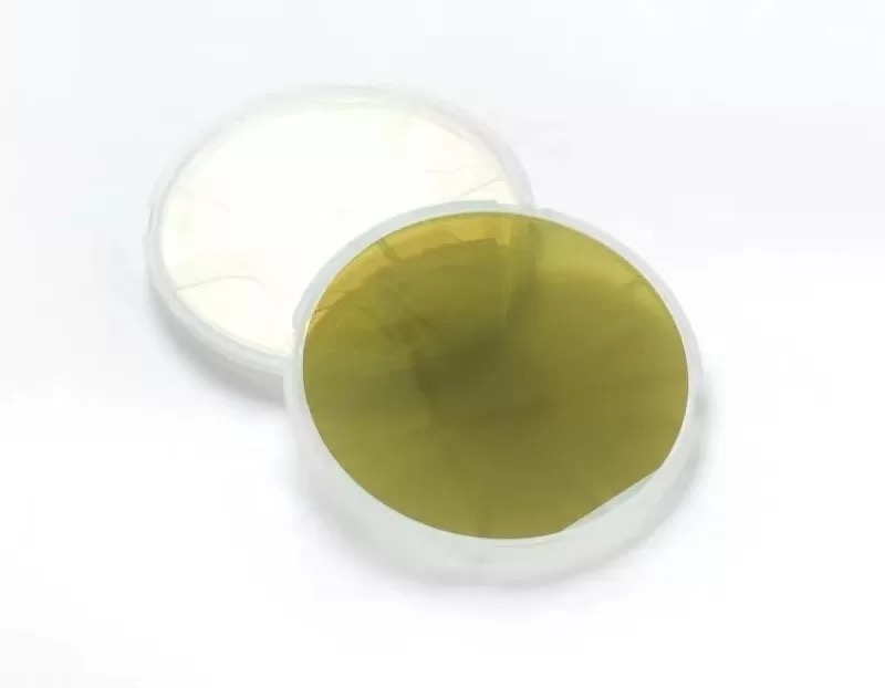
Silicon Carbide (SiC) substrates have become pivotal in advancing power electronics, particularly for Insulated Gate Bipolar Transistors (IGBTs). Their superior thermal conductivity, high breakdown voltage, and efficiency outperform traditional silicon, making them ideal for high-power applications. The 6-inch 4H N-Type SiC wafer exemplifies modern semiconductor innovation, while Dummy Grade variants streamline manufacturing processes.
Technical Specifications of 6-Inch 4H N-Type SiC Wafers
Size & Polytype:
6-inch diameter increases die yield by 2.5x vs. 4-inch wafers, reducing production costs.
4H-SiC polytype offers superior electron mobility (900 cm²/Vs) and thermal conductivity (490 W/m·K).
N-Type Doping:
Nitrogen-doped for carrier densities of 1e18–1e19 cm⁻³, optimizing conductivity for high-voltage applications.
Production Grade:
Low defect density (<0.5 cm⁻²) ensures reliability for automotive and industrial IGBTs.
Complies with SEMI standards for thickness uniformity (±10 µm) and surface roughness (<0.2 nm Ra).
Dummy Grade:
Used for equipment calibration, process testing, and R&D, minimizing waste of high-cost Production Grade wafers.
Manufacturing Processes and Challenges
Crystal Growth:
Physical Vapor Transport (PVT): Grows 4H-SiC ingots at >2,000°C, requiring precise thermal control to minimize defects like micropipes.
Chemical Vapor Deposition (CVD): Deposits epitaxial layers for tailored doping and surface quality.
Defect Management:
Advanced polishing (CMP) and AI-driven process control mitigate basal plane dislocations (BPDs) and stacking faults.
Cost Efficiency:
Transitioning to 6-inch wafers cuts costs by ~30%, though initial capital for equipment upgrades remains high.
Applications in Power Electronics
Electric Vehicles (EVs):
SiC-based IGBTs enhance inverter efficiency by 10–15%, enabling faster charging (800V systems) and extended EV range.
Renewable Energy:
Solar inverters and wind converters leverage SiC’s high-voltage tolerance (>1,700V) for grid stability.
Industrial Systems:
High-frequency IGBTs reduce energy loss in motor drives and data center power supplies.
5G Infrastructure:
Semi-insulating SiC substrates support low-loss RF devices for 5G base stations.
Role of Dummy Grade SiC Wafers
Process Calibration: Test epitaxial growth and lithography parameters without using premium substrates.
Equipment Validation: Validate diamond wire saws and plasma etchers for slicing and patterning.
Training & Prototyping: Enable engineers to refine processes cost-effectively.
Market Trends and Future Outlook
EV Dominance: EVs drive ~60% of SiC demand, with the market projected to reach $6B by 2027 (Yole Développement).
8-Inch Transition: Leaders like Wolfspeed aim to produce 8-inch wafers by 2025, further reducing costs.
Hybrid Solutions: SiC/Si hybrid modules balance performance and affordability for consumer electronics.
Conclusion
The 6-inch 4H N-Type SiC Production and Dummy Grade wafers are revolutionizing power electronics, offering unmatched efficiency for IGBTs in EVs, renewables, and industrial systems. While manufacturing challenges persist, advancements in defect control and scaling are driving adoption. As industries prioritize sustainability, SiC will remain central to the future of high-performance electronics.