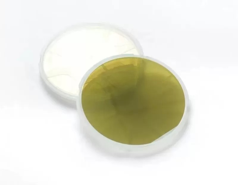
Silicon Carbide Substrate 8-Inch Production/Dummy Grade N-Type 4H-SiC Wafer for IGBT: Revolutionizing High-Power Electronics
Introduction
The shift toward high-efficiency power electronics demands materials that outperform traditional silicon. The 8-inch N-Type 4H-SiC Substrate (Production and Dummy Grade) is at the forefront of this revolution, offering superior thermal conductivity, voltage tolerance, and scalability for Insulated Gate Bipolar Transistors (IGBTs). This article delves into the production challenges, technical advantages, and transformative applications of these substrates in next-generation energy systems.
Key Features of 8-Inch N-Type 4H-SiC Substrates
4H-SiC Polytype Superiority
High Carrier Mobility: 4H-SiC’s hexagonal structure enables electron mobility ~2x higher than 6H-SiC, enhancing IGBT switching efficiency.
Thermal Conductivity (490 W/m·K): Dissipates heat 3x faster than silicon, critical for high-power applications.
N-Type Doping Precision
Nitrogen-doped substrates achieve carrier densities of 1e18–1e19 cm⁻³, optimizing conductivity for high-voltage IGBTs (up to 3.3kV).
Large Diameter, High Yield
8-inch (200mm) wafers increase die count by 56% vs. 6-inch, reducing production costs by ~35%. Production-grade quality ensures <0.5 cm⁻² defect density.
Dummy Grade Utility
Non-product grade wafers calibrate epitaxial reactors and lithography tools, minimizing wear on premium substrates and cutting R&D costs.
Applications in IGBT Technology
Electric Vehicle (EV) Inverters
SiC IGBTs boost inverter efficiency by 10–15%, extending EV range and enabling ultra-fast 800V charging systems.
Renewable Energy Converters
Solar/wind systems leverage 4H-SiC’s high breakdown voltage (>1,700V) for efficient DC-AC conversion.
Industrial Motor Drives
High-frequency SiC IGBTs reduce energy loss in industrial automation and data center UPS systems.
Rail and Smart Grids
Compact SiC modules enable lightweight traction systems and high-voltage direct current (HVDC) transmission.
Production Challenges & Innovations
Crystal Growth Complexity
Challenge: Growing defect-free 8-inch 4H-SiC ingots via PVT requires temperatures >2,200°C and precise thermal gradients.
Solution: AI-driven process control and advanced seed crystal designs suppress micropipes and basal plane dislocations.
Doping Uniformity
Challenge: Achieving consistent nitrogen distribution across 8-inch wafers.
Solution: In-situ gas flow optimization and multi-zone CVD reactors.
Cost-Effective Scaling
Challenge: High capital costs for 8-inch SiC production lines.
Solution: Partnerships (e.g., Wolfspeed & GM) to share R&D costs and standardize processes.
Role of Dummy Grade 4H-SiC Wafers
Process Calibration
Test epitaxial growth, lithography, and etching parameters without wasting high-cost production-grade wafers.
Equipment Validation
Validate 8-inch tooling (e.g., diamond wire saws) for slicing and polishing processes.
Training & Prototyping
Enable engineers to refine doping and defect inspection techniques.
Market Trends & Future Outlook
EV-Driven Demand
The EV sector accounts for 65% of SiC demand, with 8-inch wafers projected to reduce IGBT module costs by 40% by 2030.
Government Initiatives
U.S. CHIPS Act and EU’s Horizon Europe fund 8-inch SiC fabs to counter China’s 70% market share in raw SiC.
Next-Gen Innovations
Hybrid SiC/Si IGBTs and monolithic integration for consumer electronics and AI data centers.
Conclusion
The 8-inch N-Type 4H-SiC substrate and Dummy Grade wafers are pivotal in advancing high-power IGBT technology, offering unmatched efficiency for EVs, renewables, and industrial systems. While production challenges persist, innovations in crystal growth and process optimization are driving cost reductions and scalability. As global industries prioritize sustainability, SiC will solidify its role as the backbone of next-generation power electronics.